
A Broadband Millimeter-Wave Dual Polarized Phased Array for Radar Front End Applications
Design Goals:
- Compact Phased Array System
- Multibeam Capabilities
- Independent Polarization Control
- Ease of Integration
- Robust and Low Cost
- Broadband, 34 to 40 GHz
- High Resolution Imaging
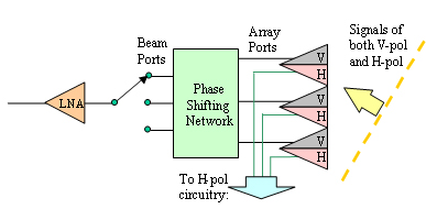
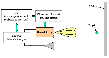
System Configuration for Receiver:
- Individual circuitry for the vertical and horizontal polarizations allow for independent control.
- Dual polarized horn antennas with orthogonal fed waveguides to discriminate the polarization.
- Rotman lens serves as phase shifting network.
- Beam control circuitry consisting of switches and LNA.
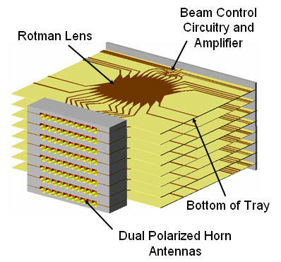
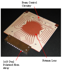
Phased Array Architecture:
- Low profile tray configuration.
- Independent control of horizontal and vertical polarizations through the top and bottom of the trays.
- Double sided tray architecture.
- 1×10 linear array of horn antennas is connected to the 10 array ports of the Rotman lens.
- Attenuating absorbing ports on sides of lens.
- Eight beam ports are connected to the SP8T PIN diode switch with LNA.
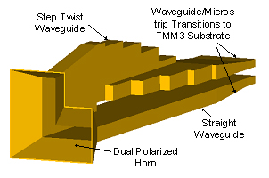
Miniature Horn Antenna Design with Waveguide Feeds:
- Waveguide and horn sections fabricated through stereolithography.
- L-shaped waveguide for vertical polarization.
- Straight waveguide for horizontal polarization.
Radar Detection Processing:
- Concurrent communication to/from the microcontroller, PC, and the network analyzer.
- Microcontroller provides the necessary TTL voltages to the comparators for the beam controlling circuitry.
- High resolution due to the broadband capabilities of the phased array.
- Through electronically controlled beam steering, the responses for each beam are processed to form a two dimensional image.
- Additional phase information from each tray allows for the formation of a three dimensional image.
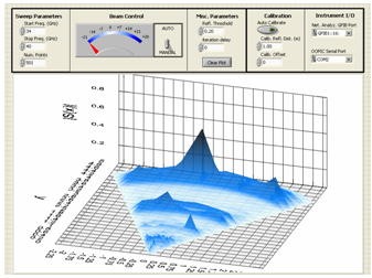
Real Time Scanning of Scene:
- Targets of different radar cross sectional areas placed at various locations.
- Image is updated after sweeping through all beam angles.
Low Phase Noise Oscillators for Wireless Applications
Introduction
During the last decades, we have witnessed rapid progress and growth in wireless communication technology and markets. This innovation not only has provided easy access to communication and information through cell phones and wireless LAN but also is opening new possibilities for improving health care and transportation safety, along with exploring unknown world such as space and deep sea. Along with the recent rapid growth, wireless communication systems have demanded wider bandwidth for faster data transmission in order to handle multimedia data as well as voice data. To address this issue, the development of a high-performance wireless transmitter and receiver (transceiver) system has been accelerated in electrical engineering.
Oscillators are key building blocks in communication transceivers. In a transceiver, oscillators generate reference sinusoidal signals for modulation and demodulation. The key issue in the oscillator design is how to minimize phase noise, which is caused by noise from active device and passive components and is a measure of the spectral purity of the oscillator signal. As shown in Fig. 1, the existence of phase noise broadens the output power spectrum of an oscillator around the carrier frequency.
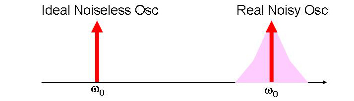
Fig.1. Oscillator Frequency Spectrum
Oscillator phase noise in wireless transceivers limits the overall performance of communication systems in a variety of ways. Phase noise directly affects short-term frequency stability, bit-error-rate, and adjacent channel interference. In wireless receivers, the phase noise of a strong adjacent channel signal interferes with a desired weak signal, thereby degrading the ultimate signal-to-noise ratio. Phase noise in wireless transmitters can also overwhelm the adjacent weak channels. Such degradations due to phase noise compromise the overall communication capability and put the stringent requirement on the performance of other transceiver blocks such as the noise figure of low noise amplifiers and the output power of power amplifiers . Since the number of wireless subscribers and thus, the amount of RF interference continue to increase, modern communication standards demand better phase noise performance from local oscillators in transceivers.

Fig. 2. The effect of phase noise on receiver systems
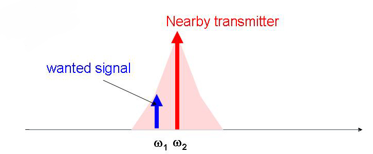
Fig. 3. The effect of phase noise on transmitter systems
In response to the above technology needs, my current research intends to demonstrate novel low phase noise oscillators. In particular, my research focuses on the development of multiple-device oscillators with low phase noise performance. In multiple-device oscillators, high-order circuit networks can be constructed with multiple transistors and passive components. The main idea of this research is to design low phase noise oscillators utilizing the mutual interaction between multiple devices and their interconnecting components in the high-order circuit network. This high-order circuit network has a number of circuit variables and can be modeled by complicated circuit equations. By manipulating the high-order circuit variables and equations, the best for low phase noise design can be found. Therefore, I am working on obtaining the optimal solutions in the high-order circuit network for specific types of multiple-device oscillators.
Low phase noise multiple device oscillator based on extended resonance technique
A novel low phase noise design technique has been proposed for power combining multiple-device oscillators. The new multiple oscillator utilizes the extended resonance technique for power combining. This technique compactly and effective places multiple solid state power devices in shunt. The extended resonance circuits are very compact since they eliminate the need for matching circuits for the individual devices. The novelty of the proposed oscillator circuit is that the extended resonance power combining circuit serves to lower phase noise as well as combine powers from multiple transistors. The solution for phase noise improvement in the oscillator is obtained by transforming the active device’s impedance, based on a well-formulated high-order circuit analysis. The experimental result shows that the designed four-device oscillator at 6GHz shows approximately 160 times phase noise improvement over a single-device oscillator, whereas the phase noise reduction of a conventional four-device oscillator is only 4 times better than a single-device one.
[1] J. Choi, A. Mortazawi, “A novel low phase noise multiple-device oscillator
based on the extended resonance technique,” in IEEE MTT-S Int. Microwave
Symp. Dig. , San Francisco , CA , June 2006. (accepted)
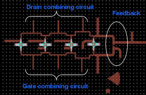
Fig. 4. Four-device Extended Resonance Oscillator Layout
Design of push- and triple-push oscillators for reducing 1/f noise upconversion
In this work, 1/f noise upconversion in push-push and triple-push oscillators was investigated and the design requirements for minimizing 1/f noise upconversion have been presented. The low frequency 1/f noise plays a dominant role in determining the close to carrier phase noise performance in oscillators. It is well known that 1/f noise is upconverted to the carrier frequency, resulting in a 1/f^3 region near the carrier frequency. 1/f noise upconversion is strongly dependent on the symmetry property of the oscillation waveform, according to a time-varying phase noise model. In push-push oscillators, the presence of the large second harmonic components may degrade the waveform symmetry of the oscillation waveforms, leading to the significant 1/f noise upconversion. To minimize 1/f noise upconversion in push-push oscillators, the phases of Fourier coefficients of all harmonics need to be equal. In triple push oscillators, the waveform symmetry can easily be achieved by eliminating all even harmonic components. The experimental results show that around 15 dB phase noise improvement at 100 kHz offset frequency can be obtained by satisfying the waveform symmetry condition in push-push and triple push oscillators. This work is the first reported approach that takes advantage of harmonic waveforms naturally generated in push-push and triple-push oscillators to optimize their phase noise performance. My work on this novel design technique resulted in my receiving a student paper award in 2005 IEEE MTT-S International Microwave Symposium.
[1] J. Choi, A. Mortazawi, “Design of push-push and triple-push oscillators for
reducing 1/f noise upconversion,” IEEE Trans. Microwave Theory & Tech., vol. 53,
no.11, pp. 3407-3414, Nov. 2005.
[2] J. Choi, A. Mortazawi, “Design of push-push oscillators for reducing 1/f noise
upconversion,” in IEEE MTT-S Int. Microwave Symp. Dig. , Long Beach, CA,
June 2005, pp. 1531-1534.
Coupled Oscillator Array for Solar Power Transmission Systems

Fig. 1. Imaginary photo of a solar power transmission satellite system
The demand for power usage will increase at least 2.5 times in the next 50 years, according to a prediction. Based on the need for clean, non-polluting sources of energy, and a trend to abandon nuclear power generation, the solar power source appears to be an attractive alternative energy source. However, earth-based solar cell power generation would require an unrealistically large earth surface area (about 1/5 of the entire United States). Instead, the concept of solar power satellite (SPS) systems has been presented so as to solve this problem. One of the key technologies for the SPS system is the wireless power transmission system, which includes DC to RF converters in the transmitters, the retrodirective beam control system and the receiving rectenna system. In this work, the overall transmitting system has been analyzed in a system perspective.
The techniques for generating and transmitting a high intensity microwave beam for solar power transmission can be divided into the centralized and the distributed approaches. The centralized approach relies on microwave tubes that are capable of generating kilo-Watts of power at microwave frequencies. However, microwave tubes are heavy, require extensive cooling system, are not as reliable as solid state devices, and therefore the system is prone to single point failure.
A more practical approach for solar power transmission via microwaves is to adopt a distributed approach with high power solid-state devices. The distributed approach will provide a lightweight, fault-tolerant system. Moreover, it will not need active cooling systems and power distributed networks. In this approach, the dc power collected from solar cells would be converted into the form of RF power using a distributed oscillator array employing high power and efficient oscillators. Microstrip patch antenna arrays with low cost and profile would transmit the converted microwave power to the earth.
This work addressed the theoretical and practical aspects of designing a very large, low profile, printed, self-oscillating injection locked active antenna array to generate a powerful coherent microwave beam. For the overall transmitting system, a beam scanning scheme to direct the microwave beam to a precise target area was presented. For the design of the coherent and stable coupled oscillator array, the extended resonance approach was considered in conjunction with the external injection locking technique.
[1] J. Choi, A. Mortazawi, “Free-space power combining oscillator array for solar power transmission,” Radio Science Bulletin, no. 311, pp.47-54, Dec. 2004. [PDF]
[2] J. Choi , A. Mortazawi and D. Pavlidis, “An approach for solar power conversion to high RF power for wireless transmission,” Invited Talk, presented in Japan-United States Joint Workshop on Space Solar Power System (JUSPS’03) , Kyoto University, 2003 [PDF]
Fig. 2. Proposed schematic of the subharmonic injection locked large array containing numerous active antenna-oscillator subarrays
Broadband Power Amplifier using Extended Resonance Technique
In previous published papers, several narrow-band multiple-device power amplifiers based on an extended resonance power combining technique have been reported. Power combining efficiencies up to 90% have been achieved at X and Ka bands. The extended resonance technique effectively places devices in shunt to combine the power from each active device. Since the magnitude of the voltage at each transistor is the same, the gain of the extended-resonance combining amplifier with N active devices is equal to the gain of a single-device amplifier, while its power capability is increased by N times. The significance of extended resonance technique lies in its ability to equally divide and combine the power of many devices using short length of transmission lines. The resulting circuits have compact layouts and are suitable for monolithic integration. However, due to these design’s resonant nature, their 3-dB bandwidth is limited to 5%. It is the purpose of this work to demonstrate an extended-resonance combining based amplifier with broadband performance.
As shown by Carlin and others, when one port of a two-port lossless lumped-element network is terminated with pure resistive load, this network’s layout can be determined from the rational function of the input Thevenin impedance (Zq=Rq+jXq) or admittance (Yq=Gq+jBq) at the other port. Another important theory about the lossless lumped-element network is that the rational function of Zq and Yq can be derived from their real parts Rq and Yq functions respectively by using Brune-Gewertz method. For lossless and reciprocal network N, through some simple derivations, it can be shown that the A and B elements of the network’s transfer matrix are directly related with its Gq function. Therefore, when the complex admittances
(G2(f)+jB2(f)) are known, the values of A and B can be determined. Then based on A and B, we can determine the network’s Gq function, and accordingly derive the rational function of Yq. In this way, the optimized lumped-element network layout with equal voltage distribution over the bandwidth of interest can be obtained. For the combining circuit presented in this paper, four-element low-pass ladder networks have been used.
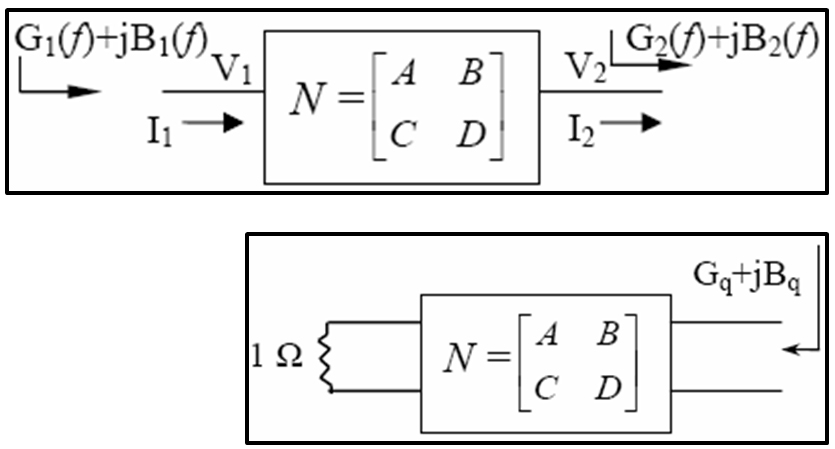
Fig. 1. Two port network
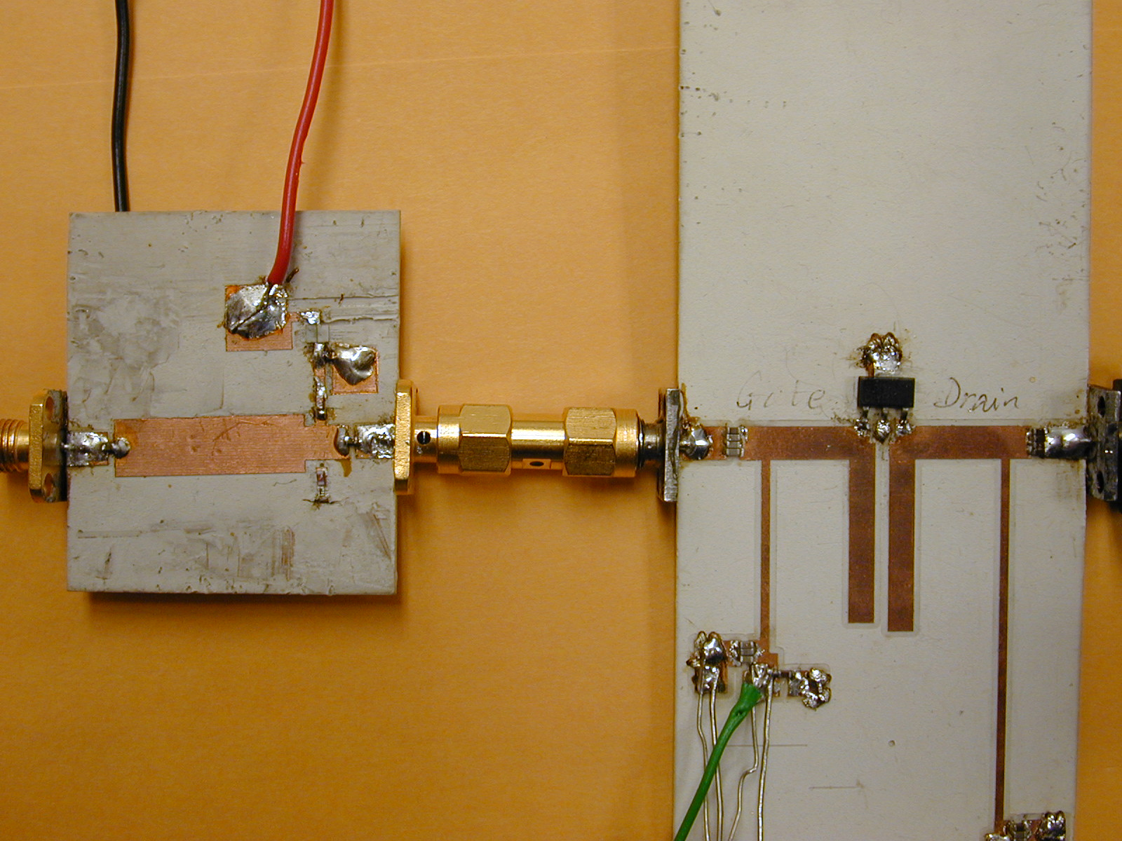
The designed 4-device broadband power amplifier was fabricated on Rogers’s 25-mil-thick TMM6 and placed on an aluminum block that also served as a heat sink. The shunt capacitors with values smaller than 0.5 pF were realized by microstrip open-end stubs and radial stubs, while the larger capacitances were achieved by using single layer chip capacitors from Dielectric Laboratories Inc. Via-holes filled with 10-mil copper wires and multiple 1-mil aluminum bonding wires were used to connect the chip capacitors to the ground. Figure shows the perspective view of the fabricated 4-device amplifier with an enlarged view of the PHEMT transistor LP1500. The gate, drain and source of the transistor were respectively connected to the RF circuits and the ground through 1-mil aluminum bonding wires. Large signal measurements were performed on both power amplifiers from 3 to 10 GHz. The measured output power levels at 1-dB gain compression (Pout@1dB) over the bandwidth are plotted. The Pout@1dB from the single-device PA is multiplied by 4 times to illustrate the possible power level from an ideal combiner. The measured Pout@1dB from our design is around 31.9 dBm with 1-dB fluctuation from 4 to 9 GHz. A comparison of these data indicates the PCE for our design is around 90% from 5 to 9 GHz.
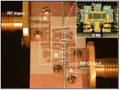
Fig. 2. Power Amplifier
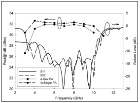
Fig. 3. Output power @1dB
Resonator-Based Predistortion Linearizer
MOBILE communication devices have become quite common in today’s world. With the increasing need to effectively utilize bandwidth, and have efficient and compact devices, the linearization of power amplifiers has become an important issue. In order to operate with high efficiency, power amplifiers are driven near and into compression, which results in high levels of distortion. This distortion, both AM-AM and AM-PM, manifests itself in the form of spectral re-growth, causing unwanted power leakage into other channels. Adjacent channel power ratio (ACPR) is a common figure of merit to quantify the spectral re-growth. For acceptable ACPR, power amplifiers must be operated at a power back-off. This results in lower efficiency.
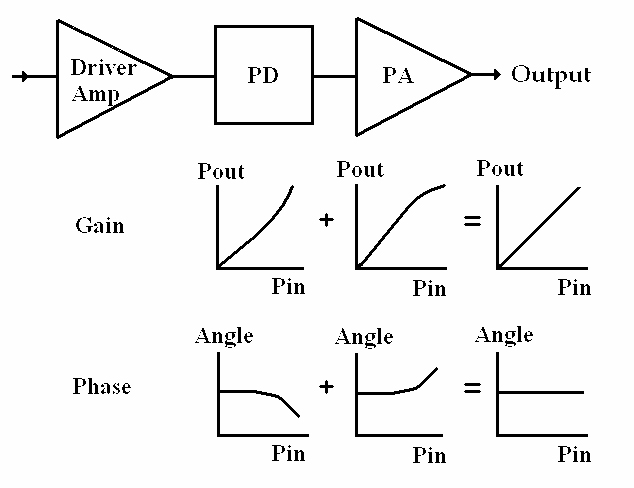
Several techniques have already been developed to linearize power amplifiers. Among these are feedback, feed-forward and predistortion. Because of their relative simplicity, compactness and modularity, predistorters (PDs) are of particular interest. A PD produces a transfer function that is the opposite of the PA’s transfer function. This results in a more linear output and lower distortion at higher power, thus the ability to operate with higher efficiency.
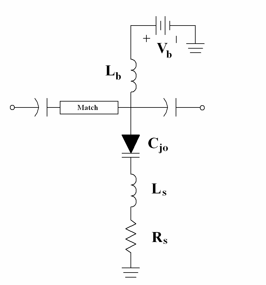
The PD is comprised of a bias network, the PD core and a quarter-wave input match. The two end capacitors are used for DC blocking. The core of the circuit is a series resonator in shunt, with a reverse biased varactor diode serving as a tunable capacitor.
The power transfer function of the PD is intimately tied to the frequency response of the resonant tank. At low power, the capacitance of the diode remains nearly constant, as dictated by the applied bias. As the RF power increases, the effective capacitance of the varactor diode also increases. This causes a shift in the phase and amplitude transfer functions. It is also possible to accomplish negative phase deviation by operating off the resonant frequency, which retains the PD circuit’s flexibility.
A PD was designed and fabricated for positive phase deviation to compensate for phase compression of the PA used. The PA was designed for operation at 1.8 GHz with 9 dB gain and 21 dBm output power.
The PD was biased at different points to demonstrate the control over the linearized PA’s transfer function and ACPR improvement. All power transfer functions were measured at 1.8 GHz. A standard NADC test signal at a carrier frequency of 1.8 GHz was used for distortion measurements, and ACPR was taken at 12.5 kHz bandwidth with 30 kHz offset. At a -2.6 V bias, the 1-dB compression point was improved from 21 dBm to 22.8 dBm with an insertion loss of 1.4 dB. The improvement in ACPR reaches a maximum of 11 dB at 17.5 dBm out for the PD biased at -3.0 V.
[1] N. Gupta, A. Tombak, and A. Mortazawi “A predistortion linearizer using a tunable resonator,” IEEE MTT-S Int. Symp. Dig.,vol. 2, pp. 6-11, June 2004.
[2] N. Gupta, A. Tombak, and A. Mortazawi “A predistortion linearizer using a tunable resonator,” IEEE Microw. Wireless Comp. Lett.,vol. 14, no. 9, pp. 431-433, Sep. 2004.
Ultra Narrow Beam Width Extended Resonance Interleaved Subarray Phase Arrays
Certain applications require phased arrays with ultra narrow beam width and moderate scan angle in the azimuth. To fulfill this stringent requirement on the beam width, conventional phased arrays impose heavy cost and complex circuitry usually unaffordable in commercial systems. Utilizing extended resonance in conjunction with the interleaved sub array technique the cost and complexity of such arrays is significantly reduced which suits them for commercial applications.
Phase shifters are considered to be the most sensitive and expensive part of a phased array. It has been estimated that almost half of the cost of a phased array is due to the cost of the phase shifters used. The extended resonance technique eliminates the need for separate power splitter and phase shifters in a conventional phased array system, and achieves power dividing and phase shifting using the same circuitry, resulting in significant amount of reduction in the circuit complexity and cost.
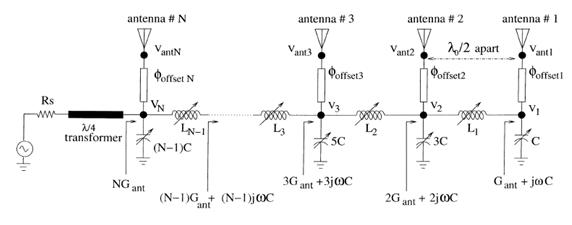
Fig.1 Extended resonance phased array concept
Furthermore the number of power dividing and combining ports can be reduced through interleaving radiating elements which also results into a compact array. Therefore the tentative structure of the arrays should look like Fig. 2.
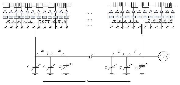
Fig. 2 Extended resonance interleaved subarray phased array
The phase shifting structure of Fig.1 fails to work if the number of phase shifting elements is large. A new circuit which is more robust to number of ports and tolerances is under further study.
‘
Turnable Microwave Component and Circuits Using Thin Film Material
No doubt that wireless communication has changed our daily life dramatically in the past decade. From simple data service, to voice service, to today’s multimedia service, the needs for more advanced functions and real time access to information is driving the technology to have multi-frequency, multi-standard, and multi-mode operation in a single hand-held device which should be kept compact and cheap. Traditional fixed frequency transceiver can’t satisfy this new trend. A reconfigurable, or tunable, transceiver has to be designed, in which tunable components like tunable capacitors (varactors), tunable inductors and tunable resistors are critical. Among them varactors are of most importance due to their wide and easy use in the circuits. Nowadays various varactor technologies exist: semiconductor varactor, micro-electro mechanical system (MEMS) and ferroelectrics.
Ferroelectrics are an interesting material whose permittivity can be varied under external static electric field. By using it as the dielectric in parallel capacitors, tunable capacitors can be achieved. Ferroelectric varactors have the merits like high capacitance tunability (~ 3:1 under 15 V), high quality factor (~100 @ 2 GHz), fast tuning speed (pico-second range), high power handling capability, low tuning voltage (5 V to 15 V) and etc. So it’s a very promising candidate for future tunable microwave circuits application.
Our research focuses on one such material called Barium Strontium Titanate (BST). We work from the material deposition, device characterization to circuits implementation, in detail: characterizing thin film ferroelectrics and varactors in microwave frequency range, design and fabrication of various tunable microwave circuits like tunable filters, phase shifters, tunable matching circuits and tunable FBARs.
1. Two Port Measurement Technique
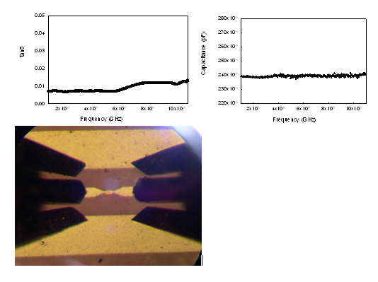
It is important to characterize thin film ferroelectric material itself first, especially at microwave frequency range. Here we proposed a simple yet accurate method to extract the permittivity and dielectric loss tangent of the thin film BST, excluding all the parasitics from the metal conductors. Three major structures were fabricated on the sapphire substrate, which are BST varactor, short standard and long standard. Two port scattering matrixes of them were measured by the vector network analyzer. Then these two port s-parameters were converted to ABCD parameters to get the complex impedances of them. By doing simple algebra among these impedances, one can extract the pure dielectric information of the thin film BST.
2. Tunable Microwave Filter
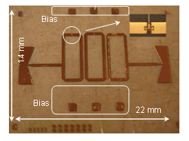
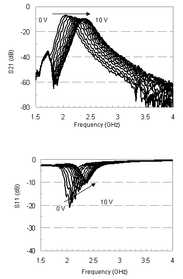
A tunable microwave filter was designed and fabricated. The building block was a capacitively loaded ring resonator which exhibited an additional zero close to the pole. This makes the filter to have a deeper roll-off skirt compared with traditional half-wavelength, quart-wavelength resonator based and combline filters. The designed center frequency was 1.8 GHz, and the fractional bandwidth was 5%. The calculated BST varactor capacitance was 0.75 pF. The measured insertion loss was about 6 dB which was due to the low quality factor of BST varactor (~40). The center frequency can be tuned from 2.0 GHz to 2.4 GHz under 10 Volts, which corresponds to 20%. During this tuning range, the fractional bandwidth of 8% was maintained.
Improving Linearity of Ferroelectric-Based Microwave Circuits
Variable capacitors (varactors) are essential components in tunable microwave circuits. Ferroelectric materials, which allow for its permittivity being adjusted by the electric field applied, are legitimate candidates for varactors. Among them, barium strontium titanate (BST) has been used in various microwave circuits, such as filters, phase shifters, and matching networks, to provide the benefit of tunability. Compared to microelectromechanical systems (MEMS) varactors, thin-film BST capacitors exhibit a higher tuning ratio under relatively low biasing voltages. However, due to the inherent nonlinear nature of the ferroelectric materials, linearity has been a concern, especially for high power applications and spectrally-packed communication systems.
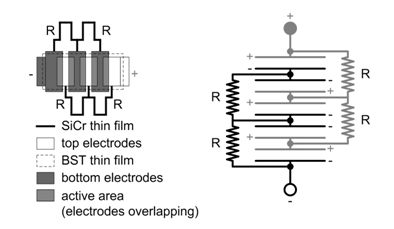
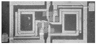
Linearity improvement can be achieved through the proper design of the device architecture, rather than changing the base material. While previous researchers have proven the effectiveness of architectural approaches for gap capacitors, in this work, a simple method to reduce the nonlinearity of parallel plate capacitors is suggested. This work presents an analysis of the technique for the study of tradeoffs and optimization of BST varactor-based circuits for wireless communication applications. The device architecture is illustrated in with a 5-stacked example. Five capacitors are connected in series through top and bottom electrodes alternatively. Thin-film resistors link together top or bottom electrodes respectively to ensure that the bias voltage falls on each capacitor equally.
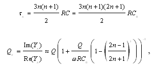
Through analysis the effects of number of stacked capacitors and the biasing resistors on the quality factor and the tuning speed of the composite capacitor are found. The time constant and the quality factor can be describe by equations respectively, where N = 2n+1 is the number of elements. The tradeoff between time constant and the degraded quality factor can be plotted versus RC0 for composite capacitors with various N‘s.
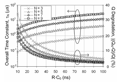
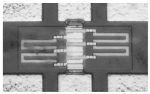
The The BST capacitors were fabricated on 430-mm-thick sapphire. The substrate has a dielectric constant of 9.39 as the electric field is perpendicular to its C-axis. The bottom electrodes composed of Ti/Au/Pt (20/2000/1000 ‘) were formed first. BST thin-film was then deposited using Pulse Laser Deposition (PLD) technique with 50/50 BST target. The measured film thickness was 400 nm. The top electrodes composed of Pt/Au (1000/2000 ‘) were then formed. After that, BST thin-film was etched in the regions other than the active area. Thin-film SiCr lines with thickness of 100 nm were then sputtered. Following that, the metal contacts composed of Cr/Au (200/500 ‘) were formed to connect the biasing resistors to the electrodes and serve as the bottom electrodes of the metal-insulator-metal (MIM) capacitors in other regions. Silicon nitride (Si3N4) thin-film, serving as the dielectric layer in the MIM capacitors and also the passivation for the BST capacitors, was deposited using Plasma Enhanced Chemical Vapor Deposition (PECVD) technique. The film thickness was measured to be 1300 ‘. Finally, the other metal traces were electroplated with gold to around 8 mm. The photograph of a 5-stacked capacitor is shown. The device area of this capacitor is 350’160 mm2, including the biasing resistors and the passivation layer. The capacitance of it is around 1.4 pF at zero bias. Various measurements are performed to demonstrate the efficacy of the technique. The 3rd order intercept point at input (IIP3) is found to be improved by 16 dB. The hot-tuning test shows that the tunability is maintained for up to 20-V peak-to-peak swing.
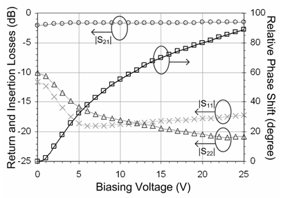
A phase shifter was designed based on all-pass network, where BST capacitors utilizing the proposed architecture with N = 5 were employed. The circuit was laid out in a flipped sense to reduce the area and facilitate cascading with other circuits. The photograph of the fabricated circuit is shown. Due to fabrication errors, the inductances of the spiral inductors were deviated from the expected value. After trimming with bond-wires, the phase shifter was measured. Its small-signal response at 2.4 GHz is shown. The insertion loss was less than 2 dB and the input and output return losses were greater than 10 dB. The relative phase shift over 0 to 25-V bias voltages was about 90 degree. The center frequency and frequency spacing of the two-tone signals for measuring the intermodulation distortion of the phase shifter were 2.4 GHz and 1 MHz, respectively. The IIP3 observed was greater than 40 dBm.
[1] J.-S. Fu, X. A. Zhu, J. D. Phillips, and A. Mortazawi, ‘Improving linearity of ferroelectric-based microwave circuits,’ IEEE Trans. Microwave Theory & Tech., vol. 55, no. 2, pp. 354-360, February 2007.
[2] J.-S. Fu, X. A. Zhu, D.-Y. Chen, J. D. Phillips, and A. Mortazawi, ‘A linearity improvement technique for thin-film barium strontium titanate capacitors,’ in 2006 IEEE MTT-S Int. Microwave Symp. Dig., June 2006.